Researchers have discovered a better way to fabricate atom-thin computer processors.
The discovery could have far-reaching impacts on nanoscale chip production and in labs across the globe where scientists are exploring 2D materials for ever-smaller and -faster semiconductors.
The researchers demonstrate that lithography using a probe heated above 100 degrees Celsius (212 F) outperformed standard methods for fabricating metal electrodes on 2D semiconductors such as molybdenum disulfide (MoS₂). Such transitional metals are among the materials that scientists believe may supplant silicon for atomically small chips.
Four advantages
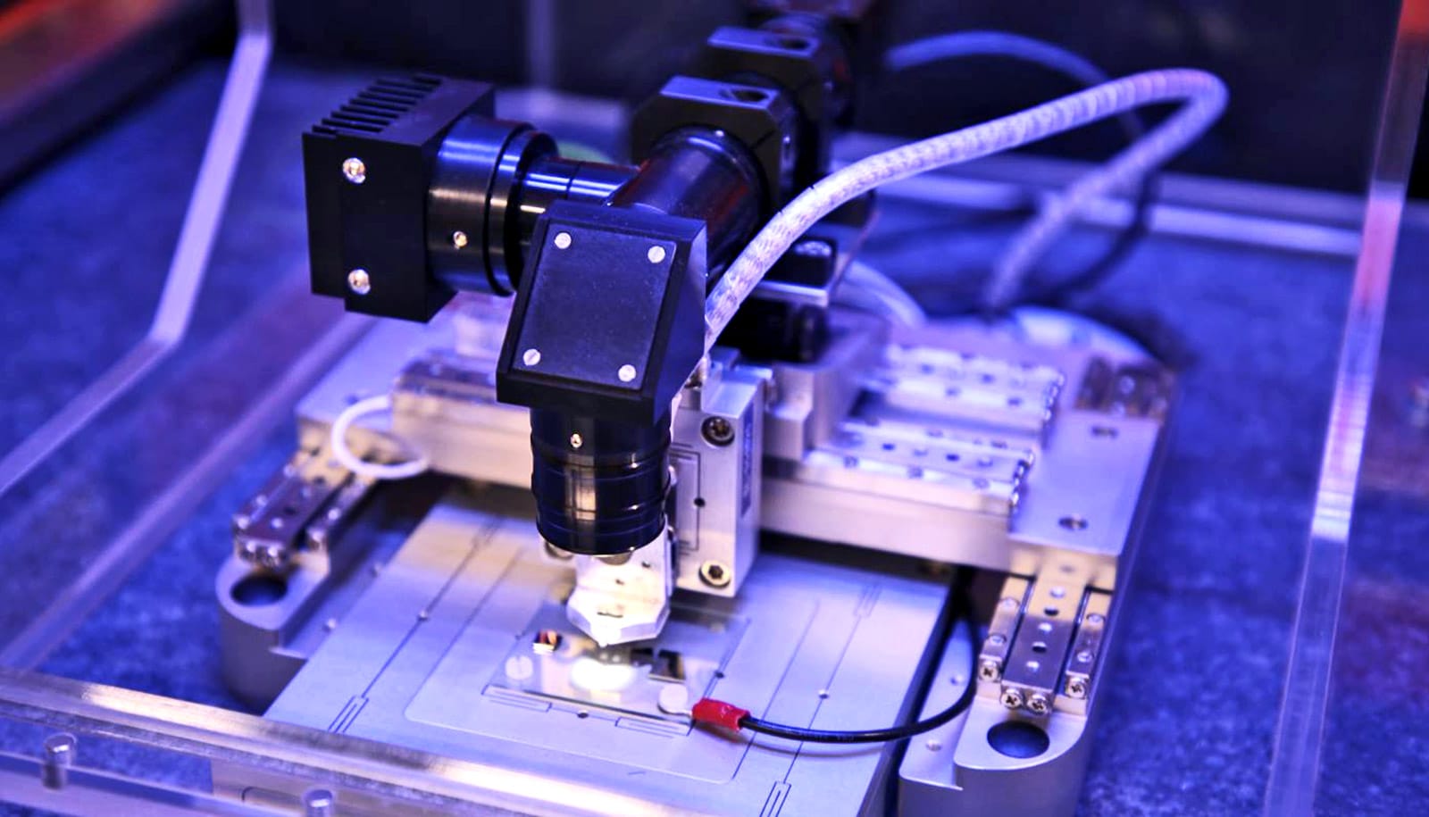
The team’s new fabrication method—called thermal scanning probe lithography (t-SPL)—offers a number of advantages over today’s electron beam lithography (EBL).
First, thermal lithography significantly improves the quality of the 2D transistors, offsetting the Schottky barrier, which hampers the flow of electrons at the intersection of metal and the 2D substrate. Second, unlike EBL, the thermal lithography allows chip designers to easily image the 2D semiconductor and then pattern the electrodes where desired.
Third, t-SPL fabrication systems promise significant initial savings as well as operational costs: They dramatically reduce power consumption by operating in ambient conditions, eliminating the need to produce high-energy electrons and to generate an ultra-high vacuum. And fourth, this thermal fabrication method can easily scale up for industrial production by using parallel thermal probes.
Out of the clean room
Elisa Riedo, professor of chemical and biomolecular engineering in the Tandon School of Engineering at New York University, hopes that t-SPL will take most fabrication out of scarce clean rooms—where researchers must compete for time with the expensive equipment—and into individual laboratories, where they might rapidly advance materials science and chip design.
The precedent of 3D printers is an apt analogy: Someday these t-SPL tools with sub-10 nanometer resolution, running on standard 120-volt power in ambient conditions, could become similarly ubiquitous in research labs like hers.
Riedo’s work on thermal probes dates back more than a decade, first with IBM Research-Zurich and subsequently SwissLitho, which former IBM researchers founded. The research team developed and used a process based on a SwissLitho system for the current work.
The team outlines the research results in Nature Electronics. Additional research contributing to the work came from NYU, Columbia University, Sungkyunkwan (Korea) University, SwissLitho, the Japanese National Institute of Materials Science, Italy’s National Research Council, and the Swiss École Polytechnique Fédérale de Lausanne.
The US Army Research Office, the Office of Basic Energy Sciences of the US Department of Energy, the National Science Foundation, and the European Union’s Horizon 2020 Research and Innovation Programme supported the research.
Source: New York University