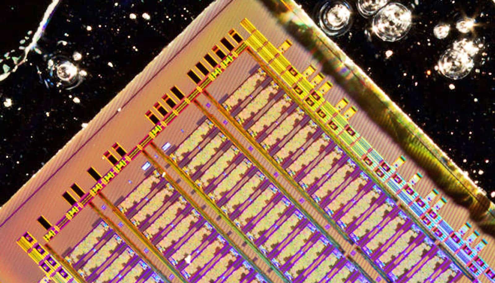
Researchers have developed a method to fabricate silicon chips that can communicate with light and are no more expensive than current chip technology.
The new microchip technology capable of optically transferring data could solve a severe bottleneck in current devices by speeding data transfer and reducing energy consumption by orders of magnitude.
“Instead of a single wire carrying around 10 gigabits per second, you can have a single optical fiber carrying 10 to 20 terabits per second…”
The electrical signaling bottleneck between current microelectronic chips has left light communication as one of the only options left for further technological progress. The traditional method of data transfer—electrical wires—has a limit on how fast and how far it can transfer data. It also uses a lot of power and generates heat. With the relentless demand for higher performance and lower power in electronics, these limits have been reached. But with this new development, that bottleneck is solvable.
“Instead of a single wire carrying around 10 gigabits per second, you can have a single optical fiber carrying 10 to 20 terabits per second—so a thousand times more in the same footprint,” says Milos Popovic, assistant professor of electrical and computer engineering at Boston University, one of the principal investigators of the study, whose team was previously at the University of Colorado Boulder where part of the work was done.
“If you replace a wire with an optical fiber, there are two ways you win,” he says. “First, with light, you can send data at much higher frequencies without significant loss of energy as there is with copper wiring. Second, with optics, you can use many different colors of light in one fiber and each one can carry a data channel. The fibers can also be packed more closely together than copper wires can without crosstalk.”
Manufacturing trouble
In the past, a manufacturing roadblock hindered progress to integrate a photonic capability onto state-of-the-art chips used in computers and smartphones. Highly developed industrial semiconductor manufacturing processes capable of stamping out a billion transistors that work together on one chip enable modern processors. But these manufacturing processes are finely tuned and designing an approach to include optical devices on chips while keeping the current electrical capabilities intact proved difficult.
The first major success in overcoming this roadblock was in 2015 when the same group of researchers published a paper in Nature that solved this problem, but in a limited commercially relevant setting.
The paper demonstrated the world’s first microprocessor with a photonic data transfer capability and the approach to manufacturing it without changing the industrial manufacturing process—a concept the researchers have termed a zero-change technology. Ayar Labs, Inc., a startup of which Popovic is a cofounder and technical advisor, has recently partnered with major semiconductor industry manufacturer GlobalFoundries to commercialize this technology.
Although this initial solution promises significant commercial impact, especially in the data communication sector, its ultimate applicability is limited because of the high cost of its starting material—silicon-on-insulator. To develop a solution for all silicon microelectronics, the researchers needed to focus their efforts on using the predominant, low-cost starting substrate—bulk silicon. Bulk silicon is used to make the majority of common microchips, and is what’s in laptops and smartphones. Silicon-on-insulator delivers a higher performance than bulk silicon, but at a significant cost premium and as such is primarily used in certain high-end microprocessors.
The perks of bulk silicon
The difference between bulk silicon and silicon-on-insulator is that the latter has a layer of insulator, typically very pure glass, directly underneath a thin layer of silicon and the former doesn’t. The glass acts as a barrier for light particles to keep them confined in optical waveguides in the device. Without the glass barrier, the light signal would be lost.
How to mass produce chips only 3 atoms thick
In the most recent paper, also published in Nature, the researchers present a manufacturing solution by introducing a set of new material layers in the photonic processing portion of a bulk silicon chip. They demonstrate that this change allows optical communication with no impact on electronics.
By working with industrial semiconductor manufacturing researchers at the Colleges of Nanoscale Science and Engineering of the State University of New York at Albany to develop this solution, the scientists ensured that any process that was developed could seamlessly become part of current industry-level manufacturing.
The result completes a several-year-long project that Vladimir Stojanovic, associate professor of electrical engineering at UC Berkeley initially led. More recently Rajeev Ram, professor of electrical engineering at MIT, has led the work. Stojanovic and Ram are Popovic’s collaborators on the project.
“By carefully investigating and optimizing the properties of the additional material layers for photonic devices, we managed to demonstrate state-of-the-art system-level performance in terms of bandwidth density and energy consumption while starting from a much less expensive process compared to competing technologies,” says Fabio Pavanello, a former postdoctoral associate from Popovic’s research group and co-first author of the paper who led the photonic transmitter device design and chip assembly in the project.
The new platform, which brings photonics to state-of-the-art bulk silicon microelectronic chips, promises faster and more energy-efficient communication that could vastly improve computing and mobile devices. Applications beyond traditional data communication include accelerating the training of deep-learning artificial neural networks used in image and speech recognition tasks, and low-cost infrared LIDAR sensors for self-driving cars, smartphone face identification, and augmented reality technology.
In addition, optically enabled microchips could enable new types of data security and hardware authentication, more powerful chips for mobile devices operating on fifth-generation (5G) wireless networks, and components for quantum information processing and computing.
DARPA funded the work.
Source: Liz Sheeley for Boston University