Researchers have demonstrated a new technique for directly printing electronic circuits onto curved and corrugated surfaces.
The work paves the way for a variety of new soft electronic technologies, and researchers have used the technique to create prototype “smart” contact lenses, pressure-sensitive latex gloves, and transparent electrodes.
“There are many existing techniques for creating printed electronics using various materials, but limitations exist,” says Yong Zhu, corresponding author of a paper on the work. “One challenge is that existing techniques require the use of polymer binding agents in the ‘ink’ you use to print the circuits. This impairs the circuit’s conductivity, so you have to incorporate an additional step to remove those binding agents after printing.
“A second challenge is that these printing techniques typically require you to print on flat surfaces, but many applications require surfaces that aren’t flat,” says Zhu, professor of mechanical and aerospace engineering at North Carolina State University.
“We’ve developed a technique that doesn’t require binding agents and that allows us to print on a variety of curvilinear surfaces,” says Yuxuan Liu, first author of the paper and a PhD student at NC State. “It also allows us to print the circuits as grid structures with uniform thickness.”
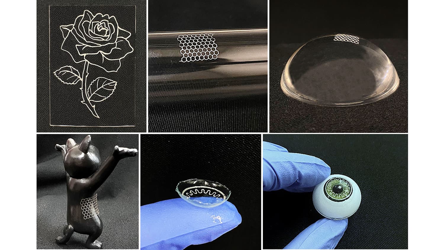
The first step in the new technique is to create a template for the relevant application that incorporates a specific pattern of microscale grooves. The template is then used to replicate that pattern in a thin elastic polymer film. Researchers then attach the thin polymer film to the relevant substrate, which can be flat or curved. At this point, the tiny grooves in the polymer are filled with a liquid solution containing silver nanowires. The solution is allowed to dry at room temperature, leaving behind silver nanowires in a soft material with the desired shape and circuit pattern.
To demonstrate the technique, the researchers created three proof-of-concept prototypes. One was a “smart” contact lens with built-in circuits, which could be used to measure the fluid pressure of the eye—which is relevant for some biomedical applications. One was a flexible, transparent electrode with circuits printed in a grid pattern, which could be used in solar cells or on touch panels. The third is a latex glove that has circuits printed on it that serve as pressure sensors, which has applications in robotics and human-machine interface applications.
“We think this could be scaled up pretty easily, in terms of manufacturing,” Zhu says. “We’re open to talking with industries who are interested in exploring this technique’s potential.”
The paper appears in the journal Science Advances. The National Science Foundation supported the work.
Source: NC State